About us
FASTPCBA Co.,Ltd
-
 Building 1, Senyang Electronic Technology Park, Guangming High-tech Park, Yutang Street, Guangming District, Shenzhen City.
-
 F:86-13418481618
-
 pcba13@fastpcba.cn
 date:2019-12-23 11:47:56
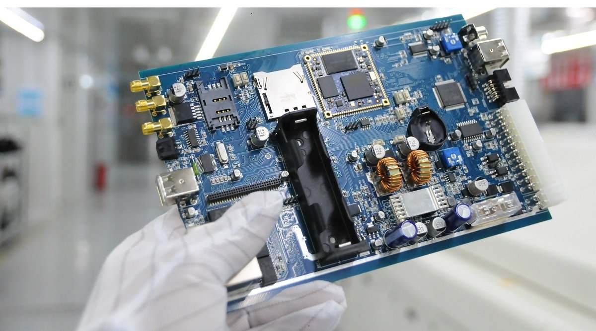
Many people have heard of the acronym "PCB" in English. But what does it mean? In fact, it is very simple. It is a printed circuit board (PCB), which is a provider of electrical connections for electronic pcb manufacturing components. Its development has a history of more than 100 years; its design is mainly layout design; the main advantages of using circuit boards are greatly reducing errors in wiring and assembly, and improving automation and production labor rates. The inventor of the printed circuit board was the Austrian Paul Eisler, who used the printed circuit board in a radio unit in 1936.In 1943, Americans used the technology heavily in military radios. In 1948, the United States officially recognized the invention for commercial use.Since the mid 1950s, printed circuit board technology has only been widely adopted. PCBs have the following functions in various electronic devices.

1.Provide mechanical support for fixing and assembling various electronic pcb manufacturing components such as integrated circuits.
2. To achieve the wiring and electrical connection (signal transmission) or electrical insulation between various electronic components such as integrated circuits to provide the required electrical characteristics, such as characteristic impedance, etc.
3. Provide solder mask graphics for automatic assembly, and provide identification characters and graphics for component insertion, inspection, and maintenance.
AOI inspection: full name is Automatic Optical Inspection, automatic optical inspection
Purpose: Feedback the image to the device for processing through the principle of optical reflection, and compare with the setting logical judgment principles or data graphics to find out the fault location
Note: Because the test method used by AOI is logical comparison, there must be some shortcomings of misjudgment, so it needs to be confirmed manually.
Chemical copper (PTH), the purpose of chemical copper: the thickness of the surface is 20-40 micro inches when chemically deposited.
The purpose of one-time copper plating: to plate 200-500 microinches of copper to protect chemical copper with a thickness of only 20-40 microinches from being damaged by subsequent processes and causing holes.
Secondary copper plating : Purpose: Thicken the exposed copper surface after development to achieve the copper thickness required by the customer
Important Raw Material: Copper Ball
Tin plating: purpose: To protect the surface of secondary copper plating with a layer of tin as a protective agent during etching. -Important raw materials: pcb manufacturing solder balls
Solder Mask, commonly known as "green oil". In order to facilitate visual inspection, more green pigments are added to the main paint. In fact, the solder mask has yellow, white, and black colors in addition to green. "
A. Solder protection: Leave the through holes and pads to be soldered on the board, and cover all lines and copper surfaces to prevent short circuits caused by wave soldering and save the amount of solder.
B. Protective board: prevent moisture and various electrolytes from oxidizing the line and jeopardize electrical performance, and prevent external mechanical damage to maintain good insulation on the board surface.
C. Insulation: As the board is getting thinner and the line width and pitch are getting thinner, the insulation problem between the conductors is becoming increasingly prominent, and the importance of the insulation performance of the solder mask is also increasing
 Building 1, Senyang Electronic Technology Park, Guangming High-tech Park, Yutang Street, Guangming District, Shenzhen City.
 F:86-13418481618
 pcba13@fastpcba.cn