About us
FASTPCBA Co.,Ltd
-
 Building 1, Senyang Electronic Technology Park, Guangming High-tech Park, Yutang Street, Guangming District, Shenzhen City.
-
 F:86-13418481618
-
 pcba13@fastpcba.cn
 date:2019-12-11 11:58:38
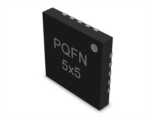
PQFN printing, mounting and rework process
The assembly process of PQFN (Plastic Quad Flat No-lead) is similar to BGA. CSP, because there is a large thermal pad on the bottom of the device, and the bottom electrode does not have the buffer function of the solder ball, so the coplanarity requirements are stricter. So it’s more difficult to assemble it than CSP

Printing and mounting of PQFN
The PQFN printing process is mainly correct stencil design. There are more stringent requirements for the height of the Z axis (mounting pressure) when mounting.
1 PQFN stencil design
It is recommended to use laser to make the stencil opening and electric filling process. Generally, the template opening size of the conductive pads around is slightly smaller than or equal to the pad size, and the stencil opening size of the large thermal pad should be reduced by 20-50%.
During reflow soldering, defects such as sputtering, solder balls, and pores are prone to occur when the gas in the thermal vias and large-area thermal pads spills out. Generally, the stencil openings for large-area thermal pads are reduced by 20% to 50%, and the solder paste coverage area is 50% to 80%. The distance between the thermal pad at the bottom of the device after PQFN soldering and the PCB thermal pad is called the device's height from the board. Practice has proved that the 50um off-plate height after PQFN welding is very helpful for heat dissipation and improving board-level reliability. In order to achieve a solder joint height of 50um, different amounts of solder paste are required for different thermal via designs.
2. PQFN printing and mountning
The printing and mounting of PQFN is similar to that of CSP. Because it cannot be visually inspected, it is required to improve the printing and mounting accuracy and select high-quality solder paste. It is recommended to choose solder powder No. 3, adopt a no-clean process, and measure the volume of solder paste by 3D SPI after printing.
The main mounting pressure (Z-axis height) during mounting. Too much solder paste or excessive mounting pressure can cause solder balls and bridges.
4. Post-weld inspection of PQFN
The post-weld inspection of PQFN is the same as that of CSP, but x-rays cannot detect the less tin and open circuit of PQFN solder joints, and can only be judged by the external solder joints.
PQFN Rework Process
The repair steps for PQFN are basically the same as the steps for repairing BGA.
A. Remove the chip: B. Clean PCB pads and component pins; C. Apply flux or solder paste D, place components E. Soldering F. Check
There are three methods for applying solder paste.
Method 1: Print a solder paste on the PCB with a repaired small screen.
Method 2: Spot solder paste on the pads of the assembly board. Spot solder paste on adjacent pads crossly to avoid solder paste adhesion.The amount of solder paste on each pad must be uniform
Method 3: The solder paste amount is directly printed on the PQFN pad in two times. Reflow once time after the first printing which is equivalent to plating a layer of tin on the pad of the PQFN. After the second printing, the PQFN is mounted on the PCB substrate for reflow. This method has a high success rate.
 Building 1, Senyang Electronic Technology Park, Guangming High-tech Park, Yutang Street, Guangming District, Shenzhen City.
 F:86-13418481618
 pcba13@fastpcba.cn