About us
FASTPCBA Co.,Ltd
-
 Building 1, Senyang Electronic Technology Park, Guangming High-tech Park, Yutang Street, Guangming District, Shenzhen City.
-
 F:86-13418481618
-
 pcba13@fastpcba.cn
 date:2019-12-12 15:10:38
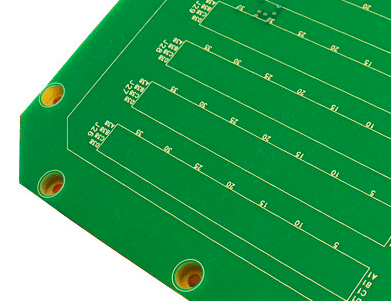
There are 4 types of holes for printed circuit boards: mechanical mounting holes, component pin insertion holes, isolation holes and via holes. This section mainly introduces the vias and the settings of vias when reflow and wave soldering processes are used.

1.Via hole
Via hole is one of the key technologies for inter-layer interconnection of multi-layer boards. Via holes are divided into through holes, buried holes and blind holes.
(1) The principle of selecting holes is to use through holes as much as possible, the second choice is buried holes, and finally blind holes. Generally, the drilling machine only has the accuracy in the two directions of x and r, and the precision of the drilling equipment for blind holes is also in the direction of the Z axis, and the precision is high, so the cost of the drilling machine is high. Holes with a diameter of less than 0.5mm are not welded, because the inner layer is easily broken after the hole is heated.
(2) hole to plate thickness ratio
It is preferred at 1: 3 and 1: 4 that 1: 5 the processing is difficult .
2, the setting of the via hole when using the reflow soldering process
A. Generally, the diameter of the via hole is not less than 0.75mm.
B. Except for SOIC. QFP or PLCC ,it is not allowed to punch through holes under other components.
C. Do not place the vias directly on the pad, the extension of the pad, or the corner of the pad.
D. There should be a thin wire coated with solder mask between the transfer hole and the pad.
3, the setting of the via hole when the wave soldering process is used
When wave soldering is used, the via should be placed at the tail of the pad or close to the pad. The position of the via hole should not be covered by the component to facilitate gas discharge. When the via hole is set on the pad, the general distance between the hole and the component head is 0.254mm.
 Building 1, Senyang Electronic Technology Park, Guangming High-tech Park, Yutang Street, Guangming District, Shenzhen City.
 F:86-13418481618
 pcba13@fastpcba.cn