About us
FASTPCBA Co.,Ltd
-
 Building 1, Senyang Electronic Technology Park, Guangming High-tech Park, Yutang Street, Guangming District, Shenzhen City.
-
 F:86-13418481618
-
 pcba13@fastpcba.cn
 date:2019-12-17 11:57:51
SMT process requirements for PCB
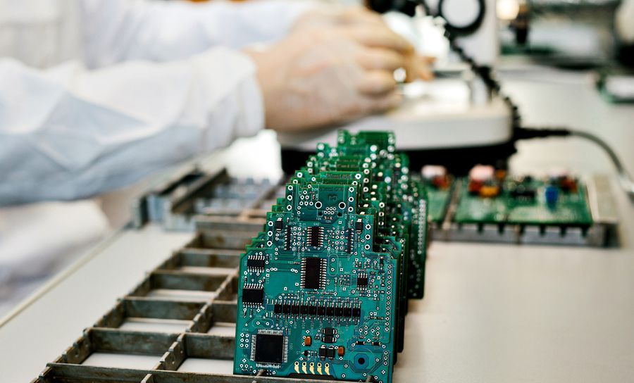
In the actual production of SMT, some customers' PCBs are designed with many devices close to the board edge, and our equipment clamping edge is made of steel, and its width is 5mm. It will cause the device to damage the board edge devices, so it is not recommended that customers have devices on the board edges. If there are devices, add process edges to protect the product.

In the actual production of SMT, there will be problems of the process side.Some companies will add the process side on the short side in order to save costs.This method of adding the process side is very dangerous. In actual production, the equipment track will be 0.5mm larger than pcb. After the PCB enters the machine, the device baffle will stop the PCB from moving, and then clamp the PCB at the clamp edge. Assuming the device baffle is the origin, the PCB actually moves to stop, and the PCB is in the actual position when the deviation of the PCB on the long-side track is small and the offset on the short-side track is large, the four corners of the PCB are easily stuck with the track, especially at the interface between the device and the device. Under normal circumstances, the part where the track joint has a gap of about 2mm, which is easy to jam. Therefore, our suggestion is to follow process edge along the long side track.If there is device near edge, add the process side on the long side.If the customer cannot add it temporarily, you need to use tooling fixtures to achieve the process side to avoid unnecessary losses.
In the actual production of SMT, many customers will encounter vias on the PCB design pads. If the vias are small, the actual SMT production may cause less tin, but not virtual soldering. This condition does not affect the function, but affects the stability of the product may prevent the device from working normally after a long time; if the via is large, it will cause less tin, and the function of the device cannot be achieved. Add solder mask between the pad and the via, otherwise tin will flow to the via.
 Building 1, Senyang Electronic Technology Park, Guangming High-tech Park, Yutang Street, Guangming District, Shenzhen City.
 F:86-13418481618
 pcba13@fastpcba.cn