About us
FASTPCBA Co.,Ltd
-
 Building 1, Senyang Electronic Technology Park, Guangming High-tech Park, Yutang Street, Guangming District, Shenzhen City.
-
 F:86-13418481618
-
 pcba13@fastpcba.cn
 date:2019-09-21 09:15:00
Basic knowledge of PCB design
Since the mid-1950s, PCB technology has been widely adopted.At present, PCB has become the "mother of electronic products", and its application is almost permeated in various terminal fields of the electronic industry, including industrial control, medical equipment, automotive electronics, smart home and many other fields.

1.Preparation
Preparing the schematic SCH component library and PCB package library before PCB design.The PCB component package library is preferably built based on the standard dimensions of the selected device.In principle, firstly build PCB component packaging library, and then build schematic SCH component library.PCB component package library requirements are high, it directly affects the installation of PCB;Schematic SCH component library requirements are relatively loose, but be careful to define pin properties and correspondence to the PCB package library.
2.PCB structure design
According to the confirmed circuit board size and various mechanical positioning, draw the PCB board frame in the PCB design environment, and place the required connectors, keys/switches, screw holes, assembly holes and so on according to the positioning requirements.Fully consider and determine the wiring area and non-wiring area (such as the extent of the area around the screw hole is a non-wiring area).
3.PCB layout design
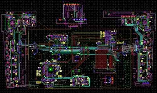
Layout design is in the PCB board frame according to the design requirements placed devices.Generate the network table in the schematic tool (Design→Create Netlist), and then Import the network table (Design→Import Netlist) in the PCB software.After the network table is successfully imported, it will exist in the background of the software. All devices can be called out through Placement operation, and there is a flying-wire prompt connection between the pins. In this case, the device layout can be designed.PCB layout design is the first important procedure in the whole design process of PCB. The more complex the PCB board is, the better the layout will directly affect the implementation difficulty of later wiring.Layout design depends on the circuit designer's basic skills and rich design experience.Junior PCB designer is inexperienced and suitable for small module layout design or PCB layout design with less difficulty.
PCB wiring design is the most workload of the whole PCB design process, which directly affects the performance of PCB board.In the design process of PCB, wiring generally has three states: the first is the layout conduction, which is the most basic entry requirements of PCB design;The second is the satisfaction of electrical performance, which is a standard to measure whether a PCB board is qualified. After the circuit layout conduction, carefully adjust the wiring, so that it can achieve the best electrical performance;Third, neat and beautiful, disorganized wiring, even if the electrical performance qualified will also bring great inconvenience to the late change board optimization and testing and maintenance , wiring require neat and uniform, not criss-cross no rules.
Layout optimization and silk-screen layout "PCB design is not the best, only better", "PCB design is an art of defects", this is mainly because PCB design need to achieve the design requirements of all aspects of hardware, and individual requirements may be in conflict, can not have both.For example, a PCB design project needs to be designed as 6 layers after the evaluation of the PCB designer, but the hardware of the product must be designed as 4 layers due to cost considerations, so the signal shielding layer can only be sacrificed, resulting in the increase of signal cross-talk between adjacent wiring layers and the decrease of signal quality.The general design rule is that it takes twice as long to optimize the wiring as it does for the initial wiring.After PCB wiring optimization is completed, post-processing is needed. The primary processing is the screen printing identification of PCB board surface. The screen printing characters at the bottom of the design need to be mirrored to avoid confusion with the screen printing at the top.
Network DRC inspection and structure inspection quality control is an important part of PCB design process, general quality control means include: design self-inspection, design mutual inspection, expert review meeting, special inspection and so on.Schematic diagram and structure element diagram are the most basic design requirements, network DRC check and structure check is two input conditions to confirm that PCB design meets of schematic diagram and structure element diagram.General circuit board designers have their own checklists of design quality, some of which are from the company's or department's specifications, and some of which are from their own experience.Special inspection includes design Valor inspection and DFM inspection, which focus on PCB design output back end processing light drawing file.
Before formal PCB processing, the PCB designer needs to communicate with the PE of the PCB manufacturer and make the manufacturer's confirmation on PCB board processing.This includes but is not limited to: PCB substrate model selection, wiring line width and distance adjustment, impedance control adjustment, PCB layer thickness adjustment, surface treatment processing technology, aperture tolerance control and delivery standards.
 Building 1, Senyang Electronic Technology Park, Guangming High-tech Park, Yutang Street, Guangming District, Shenzhen City.
 F:86-13418481618
 pcba13@fastpcba.cn