About us
FASTPCBA Co.,Ltd
-
 Building 1, Senyang Electronic Technology Park, Guangming High-tech Park, Yutang Street, Guangming District, Shenzhen City.
-
 F:86-13418481618
-
 pcba13@fastpcba.cn
 date:2021-04-02 16:38:15
What is BGA?
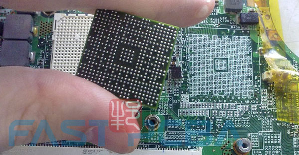
The full name of BGA is Ball Grid Array (PCB with ball grid array structure), which is a pin packaging method for large components. It is similar to the four-sided pins of QFP and is connected to the circuit board by SMT solder paste soldering. The difference is the single-row "one-degree space" pins listed around, such as gull-wing extension feet, flat extension feet, or J-shaped feet retracted to the bottom of the abdomen; change to a full array or partial array of the bottom of the abdomen, Adopt the two-dimensional area of the solder ball distribution, as a welding interconnection tool for the chip package to the circuit board. It has the characteristics of less packaging area, increased functions, increased number of pins, high reliability, good electrical performance, and low overall cost.

What is the BGA structure?
PBGA---English name is Plasric BGA, the carrier is an ordinary printed board substrate, generally a multilayer board composed of 2 to 4 layers of organic materials, the chip is connected to the upper surface of the carrier by wire bonding, and the plastic is molded. An array of eutectic solder balls is connected to the surface of the carrier.
CBGA---English name is CeramicBGA, the carrier is a multilayer ceramic, and the connection between the chip and the ceramic carrier can have two forms: wire bonding; flip chip technology. It has the advantages of excellent electrical and thermal performance and good sealing performance.
CCGA---CCGA is another form of CBGA when the size of CBGA is larger than 32*32mm. The difference is that solder pillars are used instead of solder balls. The solder column is connected by eutectic solder or directly cast and fixed on the bottom of the ceramic.
TBGA---Carrier adopts bimetallic layer tape, and chip connection is realized by flip chip technology. Can realize lighter and smaller package; suitable for I/O number can be more packaged; good electrical performance; suitable for mass electronic assembly; high reliability of solder joints.
What are the classifications of BGA?
BGA is a packaging method developed by Motorola in 1986. In the early stage, a double-sided carrier was made of BT organic sheet material to replace the traditional metal tripod for IC packaging. The biggest advantage of BGA is that the pitch is much looser than QFP. At present, the pitch of many QFPs has been tightened to 12.5mil or even 9.8mil, which makes PCB manufacturing and downstream assembly very difficult. However, if the CPU with the same function is changed to a BGA mode with a full square array of feet at the bottom of the abdomen, the foot pitch can be relaxed to 50 or 60 mils, which greatly eases the technical difficulties of upstream and downstream. At present, BGA can be divided into five categories, namely:
(1) P-BGA (double-sided and multi-layer) of plastic carrier board (BT), this type of domestic has begun mass production.
(2) C-BGA of ceramic carrier board
(3) T-BGA packaged by TAB method
(4) Ultra-small m-BGA which is only slightly larger than the original chip
(5) Other special BGAs, such as Kyocera’s D-Bga (Dimpled), Olin’s M-BGA and Prolinx’s V-BGA, etc.
The production of the outer circuit BGA:
You can make a standard BGA array according to the BGA specification and design pad size corresponding to the BGA position designed by the customer, and then use it as a benchmark to take the BGA and BGA under-holes that need to be calibrated, and back it up with the original before it is taken. Check the effect of the front and back of the shot. If the deviation between the front and rear of the BGA pad is large, it cannot be used. Only the location of the via under the BGA is shot.
BGA solder mask production:
First, the BGA surface mount solder mask window: the same as the solder mask optimization value, the unilateral window range is 1.25-3mil, and the solder mask line spacing is greater than or equal to 1.5mil; then the BGA plug hole template layer and backing board layer are processed: Make 2MM layer: copy the BGA pad of the circuit layer into another 2MM layer and process it into a square body in the 2MM range; make the plug hole layer: touch the 2MM layer with the hole layer, select Touch for the parameter Mode, and set the BGA 2MM range Copy the hole that needs to be plugged to the plug hole layer; copy the plug hole layer to another backing layer; adjust the hole diameter of the plug hole layer and the backing plate layer according to the BGA plug hole file.
In fact, due to the rapid development of electronic information products and the fierce competition in the PCB industry, the production procedures for BGA plug holes are often replaced, and new breakthroughs are constantly being made. Each breakthrough brings the product to a new level and is more adaptable to the requirements of market changes. Looking forward to more superior BGA plug holes or other processes.
 Building 1, Senyang Electronic Technology Park, Guangming High-tech Park, Yutang Street, Guangming District, Shenzhen City.
 F:86-13418481618
 pcba13@fastpcba.cn