About us
FASTPCBA Co.,Ltd
-
 Building 1, Senyang Electronic Technology Park, Guangming High-tech Park, Yutang Street, Guangming District, Shenzhen City.
-
 F:86-13418481618
-
 pcba13@fastpcba.cn
 date:2019-10-17 15:36:57
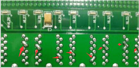
Cheap pcb manufacturing wave soldering analysis
The performances of the solder joint qualification criteria ares as follows:

1. The surface of the wave solder joint should be complete, continuous and smooth, the amount of solder is moderate, no air holes, sand holes.
2. The wettability of the solder joint is good, and it is in the shape of a crescent moon. The wetting angle of the inserted component should be smaller than 90°, preferably 15°-45°; the wetting angle of the chip component should also be smaller than 90°. The solder should be spread out at the metallized end of the chip component to form a continuous uniform coating.
3. Defects such as solder leakage, virtual welding and bridging connection should be minimized.
4. After soldering, the mounted components have no loss, and the terminal electrode does not fall off.
5. When soldering the double sided pcb, it is required that the surface of the component of the component is in good tinned.
6. After soldering, the surface of the printed board is allowed to have slight discoloration, but no serious discoloration is allowed, and the solder mask is not allowed to foam and fall off.
 Building 1, Senyang Electronic Technology Park, Guangming High-tech Park, Yutang Street, Guangming District, Shenzhen City.
 F:86-13418481618
 pcba13@fastpcba.cn