About us
FASTPCBA Co.,Ltd
-
 Building 1, Senyang Electronic Technology Park, Guangming High-tech Park, Yutang Street, Guangming District, Shenzhen City.
-
 F:86-13418481618
-
 pcba13@fastpcba.cn
 date:2021-02-22 18:19:45
Dual-in-line Package
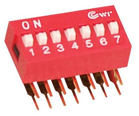
DIP—dual-in-line package, a package form of components. Two rows of leads protrude from the side of the device and are at right angles to a plane parallel to the body of the component.

The chip adopting this packaging method has two rows of pins, which can be directly soldered on a chip socket with a DIP structure or soldered in a solder position with the same number of solder holes. Its characteristic is that it can easily realize the perforation welding of the PCB board, and it has good compatibility with the main board. However, because the package area and thickness are relatively large, and the pins are easily damaged during the plug-in process, the reliability is poor. At the same time, this packaging method generally does not exceed 100 pins due to the influence of the process.
DIP package structure forms are: multilayer ceramic double in-line DIP, single-layer ceramic double in-line DIP, lead frame DIP (including glass ceramic sealing type, plastic encapsulation structure type, ceramic low-melting glass packaging type) Wait.
Single-inline Package
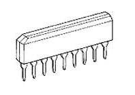
SIP—single-inline package, a package form of components. A row of straight leads or pins protrude from the side of the device.

The single in-line package (SIP) leads out from one side of the package and arranges them in a straight line. Usually, they are through-hole type, and the pins are inserted into the metal holes of the printed circuit board. When assembled on a printed circuit board, the package is side-standing. A variation of this form is the zigzag single-in-line package (ZIP), whose pins still protrude from one side of the package, but are arranged in a zigzag pattern. In this way, within a given length range, the pin density is improved. The pin center distance is usually 2.54mm, and the number of pins ranges from 2 to 23. Most of them are customized products. The shape of the package varies. Some packages that have the same shape as ZIP are called SIP.
About packaging
Packaging refers to connecting the circuit pins on the silicon chip to the external joints with wires to connect with other devices. The package form refers to the case for mounting semiconductor integrated circuit chips. It not only plays the role of mounting, fixing, sealing, protecting the chip and enhancing the electro-thermal performance, but also connects to the pins of the package shell through the contacts on the chip with wires, and these pins pass the wires on the printed circuit board. Connect with other devices to realize the connection between the internal chip and the external circuit. Because the chip must be isolated from the outside world to prevent impurities in the air from corroding the chip circuit and causing electrical performance degradation.
On the other hand, the packaged chip is also easier to install and transport. Since the quality of packaging technology also directly affects the performance of the chip itself and the design and manufacturing of the PCB (printed circuit board) connected to it, it is very important.
At present, packaging is mainly divided into DIP dual in-line and SMD chip packaging.
 Building 1, Senyang Electronic Technology Park, Guangming High-tech Park, Yutang Street, Guangming District, Shenzhen City.
 F:86-13418481618
 pcba13@fastpcba.cn