About us
FASTPCBA Co.,Ltd
-
 Building 1, Senyang Electronic Technology Park, Guangming High-tech Park, Yutang Street, Guangming District, Shenzhen City.
-
 F:86-13418481618
-
 pcba13@fastpcba.cn
 date:2019-04-29 10:28:00
In SMT circuit board assembly,PCB panel manufacturing skills

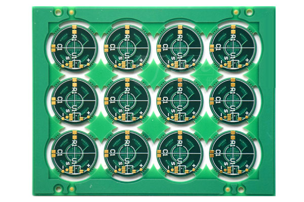
1. The outer frame (clamping edge) of the PCB panel should adopt a closed-loop design to ensure that the PCB panel will not be deformed after being fixed on the fixture;
2. PCB board width ≤ 260mm (SIEMENS line) or ≤ 300mm (FUJI line); if automatic dispensing is required, PCB board width × length ≤ 125 mm × 180 mm;
3. PCB panel as close to the square as possible, it is recommended to use 2 × 2, 3 × 3, ... panel in SMT circuit board assembly; but do not make mirrorboard);
4. The center distance between the small board is controlled between 75 mm and 145 mm;
5. When setting the fiducial mark, usually leave a non-resistive soldering area 1.5 mm larger than the fiducial mark;
6. There should be no large devices or protruding devices near the connection point between the outer frame of the panel and the inner small board, small board and small board, and the space between the components and the PCB should be more than 0.5mm. To ensure the normal operation of the cutting tool in process of SMT circuit board assembly;
7. Four positioning holes are opened at the four corners of the outer frame of the panel. The hole diameter is 4mm±0.01mm. The strength of the hole should be moderate to ensure that it will not break during the upper and lower boards. The aperture and position accuracy should be high, and the hole wall should be smooth and burr-free. ;
8. Each small board in the PCB panel must have at least three positioning holes, 3≤ aperture ≤6 mm, no wiring or mounting components is allowed within 1mm of the edge positioning hole in the process of SMT circuit board assembly;
9. The whole board positioning for PCB and the fiducial mark for fine-pitch device positioning. In principle, the QFP with a pitch less than 0.65mm should be set at its diagonal position; the fiducial mark for locating the PCB sub-board should be paired. Used, arranged at the diagonal of the positioning element in the process of SMT circuit board assembly;
10.Large components should be left with positioning posts or positioning holes, such as I / O interface, microphone, battery interface, micro switch, headphone interface, motor and so on.
 Building 1, Senyang Electronic Technology Park, Guangming High-tech Park, Yutang Street, Guangming District, Shenzhen City.
 F:86-13418481618
 pcba13@fastpcba.cn