About us
FASTPCBA Co.,Ltd
-
 Building 1, Senyang Electronic Technology Park, Guangming High-tech Park, Yutang Street, Guangming District, Shenzhen City.
-
 F:86-13418481618
-
 pcba13@fastpcba.cn
 date:2020-10-16 14:28:27
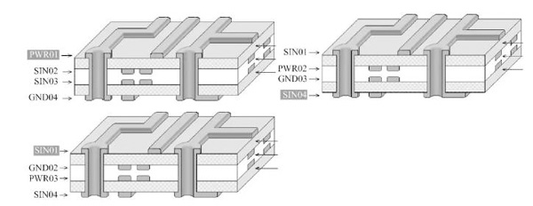
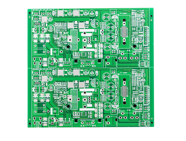
The pcb circuit board includes many types of working layers, such as signal layer, protective layer, silk screen layer, internal layer, etc. The functions of each layer are briefly introduced as follows:

1.Signal layer: mainly used to place components or wiring. Protel DXP usually contains 30 middle layers, namely Mid Layer 1 to Mid Layer 30. The middle layer is used to arrange signal lines, and the top and bottom layers are used to place components or deposit copper.
2.Protection layer: It is mainly used to ensure that the parts that do not need to be tinned on the pcb circuit board are not tinned, so as to ensure the reliability of the operation of the pcb circuit board. Among them, Top Paste and Bottom Paste are the top solder resist layer and the bottom solder resist layer respectively; Top Solder and Bottom Solder are the solder paste protective layer and the bottom solder paste protective layer respectively.
3.Silk screen layer: mainly used to print the serial number, production number, company name, etc. of the components on the pcb circuit board.
4.Internal layer: Mainly used as signal wiring layer. Protel DXP contains 16 internal layers.
5.Other layers: mainly includes 4 types of layers.
Drill Guide (drilling azimuth layer): mainly used for the position of drilling holes on the printed circuit board.
Keep-Out Layer: Mainly used to draw the electrical border of the circuit board.
Drill Drawing (drilling drawing layer): Mainly used to set the drilling shape.
Multi-Layer: Mainly used to set up multiple layers.

 Building 1, Senyang Electronic Technology Park, Guangming High-tech Park, Yutang Street, Guangming District, Shenzhen City.
 F:86-13418481618
 pcba13@fastpcba.cn