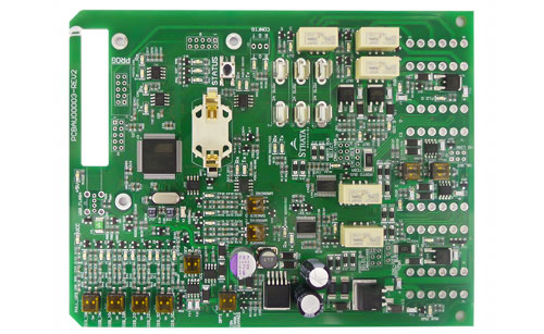
PCB board design
 date:2018-11-13 09:57:00
PCB board design
1. How to choose PCB circuit board?
Choosing PCB circuit boards must strike a balance between meeting design requirements and mass production and cost. Design requirements include both electrical and institutional components. This material problem is usually more important when designing very high speed PCB boards (greater than GHz). For example, the commonly used FR-4 material, the dielectric loss at a frequency of several GHz has a great influence on the signal attenuation, and may not be useful. As far as electrical is concerned, it is important to note whether the dielectric constant and the dielectric loss are combined at the designed frequency.

2. How to avoid high frequency interference?
The basic idea of avoiding high-frequency interference is to minimize the interference of high-frequency signal electromagnetic fields, which is called crosstalk. You can use the distance between the high-speed signal and the analog signal, or add ground guard/shunt traces next to the analog signal. Also pay attention to the digital ground noise interference to the analog ground.
3. How to solve signal integrity problems in high-speed design?
Signal integrity is basically a matter of impedance matching. The factors affecting the impedance matching are the architecture of the signal source and the output impedance, the characteristic impedance of the trace, the characteristics of the load end, and the topology of the trace. The solution is to *termination and adjust the topology of the trace.
4. How is the differential wiring method implemented?
There are two points to note for the wiring of the differential pair. One is that the length of the two lines should be as long as possible, and the other is that the spacing between the two lines (which is determined by the differential impedance) should remain the same, that is, to be parallel. There are two ways of paralleling. One is that the two lines are on the same side-by-side, and the other is two lines that are on the top-by-side. In general, the former side-by-side implementation is more.
5. How to implement differential wiring for a clock signal line with only one output?
To use differential routing, it must be meaningful that both the source and the receiver are differential signals. Therefore, differential wiring cannot be used for a clock signal with only one output.
6. Can I add a matching resistor between the differential pairs at the receiving end?
The matching resistance between the differential pair of the receiving end is usually added, and its value should be equal to the value of the differential impedance. This signal quality will be better.
7. Why is the wiring of the differential pair close and parallel?
The wiring of the differential pairs should be properly close and parallel. The proper proximity is because this spacing affects the value of the differential impedance, which is an important parameter in designing the differential pair. Parallelism is also required because the consistency of the differential impedance is maintained. If the two lines are too close, the differential impedance will be inconsistent, which will affect signal integrity and timing delay.
8, how to deal with some theoretical conflicts in the actual wiring
(1) Basically, it is correct to isolate the analog/digital divisions. It should be noted that the signal trace should not cross the moat as much as possible, and do not let the return current path of the power supply and signal become too large.
(2) The crystal oscillator is an analog positive feedback oscillator circuit. To have a stable oscillation signal, the loop gain and phase specifications must be met. The oscillation specifications of the analog signal are easily disturbed, even if the ground guard traces may not be completely isolated. interference. And too far away, the noise on the ground plane will also affect the positive feedback oscillator circuit. Therefore, the distance between the crystal and the chip must be close to possible.
(3) There are many conflicts between high-speed wiring and EMI requirements. However, the basic principle is that the electrical resistance of the EMI or the ferrite bead cannot cause some electrical characteristics of the signal to fail to meet the specifications. Therefore, it is best to use the techniques of routing and PCB stacking to solve or reduce EMI problems, such as high-speed signals going inside. Finally, use resistors or ferrite bead to reduce the damage to the signal.
9. How to solve the contradiction between manual wiring and automatic wiring of high-speed signals?
Most of the autorouters of the current wiring software have set constraints to control the winding method and the number of vias. The EDA company's winding engine capabilities and constraints are sometimes far from being set. For example, is there enough constraint to control the serpentine 蜿蜒, whether it can control the spacing of the differential pairs, and so on. This will affect whether the routing method that is automatically routed can meet the designer's ideas. In addition, the difficulty of manually adjusting the wiring is also absolutely related to the ability of the winding engine. For example, the ability to push the line, the ability to push through the hole, and even the ability to push the copper to the copper. Therefore, choosing a router with a strong winding engine is the solution.
FASTPCBA 20 years' experience for PCB Assembly.
 Building 1, Senyang Electronic Technology Park, Guangming High-tech Park, Yutang Street, Guangming District, Shenzhen City.
 F:86-13418481618
 pcba13@fastpcba.cn
 date:2018-11-13 09:57:00

 Building 1, Senyang Electronic Technology Park, Guangming High-tech Park, Yutang Street, Guangming District, Shenzhen City.
 F:86-13418481618
 pcba13@fastpcba.cn