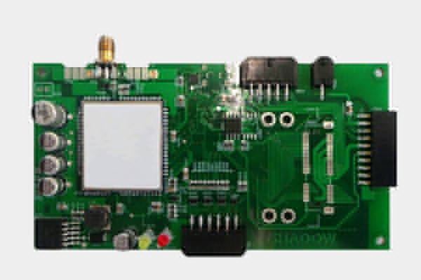
PCB component layout
 date:2018-11-16 16:48:00
PCB component layout
First, consider the PCB size. When the PCB size is too large, the printed lines are long, the impedance is increased, the anti-noise ability is lowered, and the cost is also increased; if the size is too small, the heat dissipation is not good, and adjacent lines are susceptible to interference. After determining the PCB size, understand the attribute information of each component, including electrical performance, external dimensions, pin distance, etc., and then determine the position of the component. Finally, according to the functional unit of the circuit, the layout of all the components of the circuit, need to pay attention to the following aspects:

1) The component arrangement is generally in the direction of signal flow, starting from the input stage and ending at the output stage. Each unit circuit is relatively concentrated and centered around the core device and laid out around it. Minimize the wiring between high frequency components, reduce their distribution parameters and mutual electromagnetic interference. For the arrangement of adjustable components, it is necessary to consider the adjustment. Components that are susceptible to interference cannot be placed too close together, and input and output components should be kept as far away as possible.
2) Symmetrical circuits, such as push-pull amplifiers, differential amplifiers, bridge circuits, etc., should pay attention to the symmetry of the components. As far as possible, the distribution parameters are consistent. Inductors with iron cores should be placed perpendicular to each other and away from each other to reduce mutual coupling.
3) For the layout of adjustable components such as potentiometers, adjustable inductors, variable capacitors, microswitches, etc., the structural requirements of the whole machine should be considered. If it is adjusted inside the machine, it should be placed on the printed board to facilitate adjustment; if it is adjusted outside the machine, its position should be compatible with the position of the adjustment knob on the chassis panel.
4) The components are arranged evenly, neatly and compactly, and the density is the same. Try to be horizontal and vertical as far as possible, and the components cannot be arranged obliquely or cross-rearranged. The leads between the unit circuits should be as short as possible and the number of leads should be as small as possible.
5) The components located at the edge of the board are generally not less than 2mm from the edge of the board. The distance between the outer shells of each component shall be determined according to the voltage between them and shall not be less than 0.5 mm.
FASTPCBA 20 years' experience for PCB Assembly.
 Building 1, Senyang Electronic Technology Park, Guangming High-tech Park, Yutang Street, Guangming District, Shenzhen City.
 F:86-13418481618
 pcba13@fastpcba.cn
 date:2018-11-16 16:48:00

 Building 1, Senyang Electronic Technology Park, Guangming High-tech Park, Yutang Street, Guangming District, Shenzhen City.
 F:86-13418481618
 pcba13@fastpcba.cn