Pcb configuration developer
 date:2018-11-16 16:57:00
Pcb configuration developer
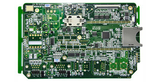
In the sensitized gap, let's configure the developer. A pack of developer has 29G, more, about 10G is enough... Prepare the developer according to the ratio of developer: water 1:20 (re-emphasize that you must use a plastic pot!) Pour the developer into the preparation. In 200 ml of water, stir and shake the container until the developer is completely dissolved and there are no more particles. Then take out the sensible circuit board and tear off the transparent glue. This should be like this.

Put the board slowly into the developer (don't throw it in). After a few seconds, you can see that the non-circuit part of the film gradually turns into a green smoke and floats out. At this point, gently shake the plastic pot until the situation shown below. . The line portion has been clearly defined, and the dark green photosensitive film in the non-line portion should also be completely dissolved. Wait another 3-5 seconds. To ensure that the imaging process is 100% complete!
Note: Used imaging fluid is strictly prohibited. Please dilute the used imaging solution 20 times before discharging it into the city's sewer system!
FASTPCBA 20 years' experience for PCB Assembly.
 Building 1, Senyang Electronic Technology Park, Guangming High-tech Park, Yutang Street, Guangming District, Shenzhen City.
 F:86-13418481618
 pcba13@fastpcba.cn
 date:2018-11-16 16:57:00

 Building 1, Senyang Electronic Technology Park, Guangming High-tech Park, Yutang Street, Guangming District, Shenzhen City.
 F:86-13418481618
 pcba13@fastpcba.cn