About us
FASTPCBA Co.,Ltd
-
 Building 1, Senyang Electronic Technology Park, Guangming High-tech Park, Yutang Street, Guangming District, Shenzhen City.
-
 F:86-13418481618
-
 pcba13@fastpcba.cn
 date:2020-12-31 15:44:08
We all know that circuit boards are made up of layers of copper foil circuits, and the connections between different circuit layers are via vias. This is because today's circuit board manufacturing uses drilled holes to connect different The circuit layer is the same as the connection channel of a multi-layer underground waterway. The difference is that the purpose of the circuit board is to energize, so a layer of conductive material must be plated on its surface so that electrons can move between them.

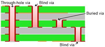
Generally, there are three types of PCB vias that we often see:
Plating Through Hole: abbreviated as PTH, this is the most common one, you only need to pick up the PCB and face the light, the hole where you can see the bright light is PTH. This is also the simplest type of hole, because when making it, you only need to use a drill or a laser to directly drill the circuit board, and the cost is relatively cheap. In contrast, some circuit layers do not need to connect these vias. So although through holes are cheap, they sometimes use more PCB space.
Blind Via Hole: refers to the via holes that connect the inner layers and are not visible on the surface of the finished board. The above-mentioned two types of holes are located in the inner layer of the circuit board, and are completed by a through-hole forming process before lamination, and several inner layers may be overlapped during the formation of the via.
The outermost circuit of the PCB is connected to the adjacent inner layer with electroplated holes. Because the opposite side cannot be seen, it is called Blind Via Hole. In order to increase the space utilization of the PCB circuit layer, the Blind Via Hole process was born. This production method requires special attention to the depth of the drilling (Z axis) to be just right. This method often causes difficulties in electroplating in the hole, so it is almost used by no manufacturer: it is also possible to place the circuit layers that need to be connected in the individual circuit layers in advance. At this time, the holes are drilled first, and then glued together, but a more precise positioning and alignment device is required.
Buried Hole: The connection of any circuit layer inside the PCB but not conducting to the outer layer. This process cannot be achieved by drilling after bonding. The drilling must be performed on the individual circuit layers. After the inner layer is partially bonded, it must be electroplated before it can be fully bonded. Compared with the original Plating Through Hole and Blind Via Hole is more time-consuming, so the price is the most expensive. This process is usually only used on high-density (HDI) circuit boards to increase the usable space of other circuit layers.
 Building 1, Senyang Electronic Technology Park, Guangming High-tech Park, Yutang Street, Guangming District, Shenzhen City.
 F:86-13418481618
 pcba13@fastpcba.cn