About us
FASTPCBA Co.,Ltd
-
 Building 1, Senyang Electronic Technology Park, Guangming High-tech Park, Yutang Street, Guangming District, Shenzhen City.
-
 F:86-13418481618
-
 pcba13@fastpcba.cn
 date:2019-10-30 17:20:47
PCB manufacturing solder paste printing quality control
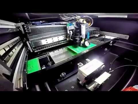
The entire pcb manufacturing printing process can be subdivided into: clamping alignment, tin filling, flattening and release. The following describes the various processes of solder paste printing and their control points.

1, Clamping alignment
The PCB enters the printing machine through the loading track. Firstly, the two sides of the track are clamped and the bottom supports the thimble mechanically. Then the optical identification system corrects the PCB and the template to ensure that the opening of the steel stencil and the pad of the PCB are accurately aligned.
Different printing machines use different PCB positioning and clamping methods. During the printing process, attention should be paid to the clamping condition of the clamping device and the PCB, especially the thin board and the large-sized PCB. Otherwise, the following problems will occur.
1) The PCB surface is not flat, causing damage to the steel stencil and the squeegee during the top printing process, or poor sticking to the steel stencil and causing the solder paste to leak and tin connection.
2) After the photo recognition of the printing machine, the offset of the PCB position during the printing process of the top pcb manufacturing leads to the printing deviation.
3) Uneven or thick thickness, a common problem in the process of clamping alignment is deviation , which leads to many factors of offsetting the solder paste. The reason for the deviation is usually the poor quality of the identification point and the illuminance of the recognition point not adjusted well, the printer actuator is worn out with reduced accuracy or the motor is not functioning properly.
2, Solder paste filling and smoothing
The squeegee drives the solder paste through the stencil, during which the solder paste rolls and is well filled. The influencing factors are related to the viscosity, shear force, particle size and stencil opening design of the solder paste, which is one of the key factors for quality control in the printing process.
3, Solder paste release
Solder paste release is the process of transferring the solder paste from the stencil opening to the PCB pad. Good release can ensure a good solder paste shape. Generally, the thinner the stencil, the larger/wider the pad. The easier it is to release, and vice versa. At present, the fine-pitch QFP, BGA stencil opening of solder paste is the bottleneck of solder paste printing.
At the time of release, there are mainly problems such as tin tip and solder paste collapse. There are many factors in the tipping and solder paste collapse, such as demoulding speed, demoulding distance, surface perferction of steel mesh side wall, and solder paste viscosity. When the solder paste is well controlled, the cause of the tipping and solder paste collapse is usually due to the poor mold release of the solder paste in pcb manufacturing, especially in the case of fine pitch, in order to improve the quality of solder paste release. Generally, there are functions of demoulding speed and demoulding distance control. In the case of fine pitch, the recommended demolding speed is: 0.1~0.3mm/s, and some machines also have vibration function to help demoulding. Increase the demoulding distance to ensure that there is a distance from the steel stencil after the demoulding is completed, and the lifting system will accelerate down, avoiding the tin tipping and solder collapse due to demoulding too fast and too early.
 Building 1, Senyang Electronic Technology Park, Guangming High-tech Park, Yutang Street, Guangming District, Shenzhen City.
 F:86-13418481618
 pcba13@fastpcba.cn