About us
FASTPCBA Co.,Ltd
-
 Building 1, Senyang Electronic Technology Park, Guangming High-tech Park, Yutang Street, Guangming District, Shenzhen City.
-
 F:86-13418481618
-
 pcba13@fastpcba.cn
 date:2020-11-12 17:56:33
In circuit board design, Via as the most basic element runs through the entire PCB. Each PCB Vias has its meaning and is designed for its purpose.
Via is an important part of multi-layer circuit boards. The cost of Drill Via usually accounts for 30%-40% of the cost of circuit board production. However, the importance of vias in PCBs is not only because of its quantity and price, but also suitable Hole size, quantity, distance between vias and vias and traces, distance between components, via capacitance, via inductance, etc. All have a certain impact on the design of a PCB with good performance.
Vias on the circuit board can be divided into two categories according to their functions:
One is for electrical connection between layers;
The second is for device fixing or positioning;
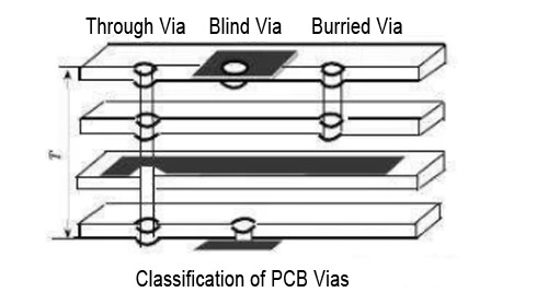
The process is divided into three categories, namely Blind Via, Burried Via and Through Via.

Blind Via is located on the top and bottom surfaces of the PCB and has a certain depth. It is used to connect the surface line and the inner line below. The depth of the Vias and the diameter of the Vias usually do not exceed a certain ratio.
Burried Via refers to the connection Vias located on the inner layer of the PCB, which does not extend to the surface of the circuit board.
Burried Via is located on the inner layer of the circuit board. It is completed by the Through Via molding process before lamination. Several inner layers may be overlapped during the formation of Vias.
Finally, regarding Through Via, this type of Via passes through the entire circuit board for internal interconnection or component installation and positioning Vias. Because Through Via is easier to implement in technology and lower in cost, most printed circuit boards use it.
From a design perspective, a via is mainly composed of two parts, one is the Drill Via in the middle, and the other is the pad area around the Drill Via. The size of these two parts determines the size of the via. Obviously, when designing high-speed and high-density circuit boards, circuit board designers always hope that Vias is as small as possible, so that more wiring space can be reserved on the circuit board; in addition, the smaller the via, the smaller its own parasitic capacitance. Suitable for high-speed circuits. But at the same time, the reduction in size has also brought about an increase in cost, and the size of vias cannot be reduced indefinitely, which is limited by process technologies such as Drill Via and Plating. The smaller the Vias, the longer it takes Drill Via and the easier it is to deviate from the center position.
 Building 1, Senyang Electronic Technology Park, Guangming High-tech Park, Yutang Street, Guangming District, Shenzhen City.
 F:86-13418481618
 pcba13@fastpcba.cn