About us
FASTPCBA Co.,Ltd
-
 Building 1, Senyang Electronic Technology Park, Guangming High-tech Park, Yutang Street, Guangming District, Shenzhen City.
-
 F:86-13418481618
-
 pcba13@fastpcba.cn
 date:2019-11-02 11:30:25
Prototype pcb manufacturing, how to control PCB and components before wave soldering?
When designing plug-in component pads, the pad size should be designed appropriately. The pad is too large, the solder spread area is large, the formed solder joint is not full, and the surface tension of the small pad copper foil is too small, and the formed solder joint is not wetted. The matching gap between the aperture and the component leads is too large, and it is easy to virtual solder. When the aperture is 0.05~0.2mm wider than the lead and the pad diameter is 2~2.5 times of the aperture, it is an ideal condition for prototype pcb manufacturing.

When designing the chip component pads, the following points should be considered:
A. In order to remove the "shadow effect" as much as possible, the soldering end or pin of SMD should face the direction of the tin flow to facilitate contact with the tin flow, reduce the virtual soldering and leakage soldering
B. The wave soldering technique is not suitable for fine pitch OFP, PLCC, BGA and small pitch SOP components, which means that such components should not be placed on the side of the wave soldering.
C. Smaller components should not be held behind a large component, so as to prevent large components from blocking the contact between the tin flow and the pads of the smaller components, resulting in leakage soldering in prototype pcb manufacturing.
2. PCB flatness control
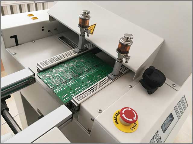
Welding has high requirement for the printed circuit board flatness. Generally, the warpage is required to be less than 0.5 mm. If it is greater than 0.5 mm, it should be leveled. In particular, some printed circuit boards have a thickness of only about 1.5 mm, and their warpage requirements are higher, otherwise the soldering quality cannot be guaranteed. Properly preserve the printed circuit boards and components, minimize the storage cycle during soldering, and avoid dust, grease, oxide copper foil and component leads to form qualified solder joints. Therefore, printed circuit boards and components should be saved in a dry, clean environment, and to minimize storage cycles. For printed circuit boards that have been placed for a long time, the surface is generally cleaned, which improves the solderability of prototype pcb manufacturing, reduces virtual soldering and bridging. For component leads that have a certain degree of oxidation on the surface, the surface oxide should be removed firstly.
 Building 1, Senyang Electronic Technology Park, Guangming High-tech Park, Yutang Street, Guangming District, Shenzhen City.
 F:86-13418481618
 pcba13@fastpcba.cn