About us
FASTPCBA Co.,Ltd
-
 Building 1, Senyang Electronic Technology Park, Guangming High-tech Park, Yutang Street, Guangming District, Shenzhen City.
-
 F:86-13418481618
-
 pcba13@fastpcba.cn
 date:2019-06-21 17:25:00
Regarding the BGA capsulation, you must read this article
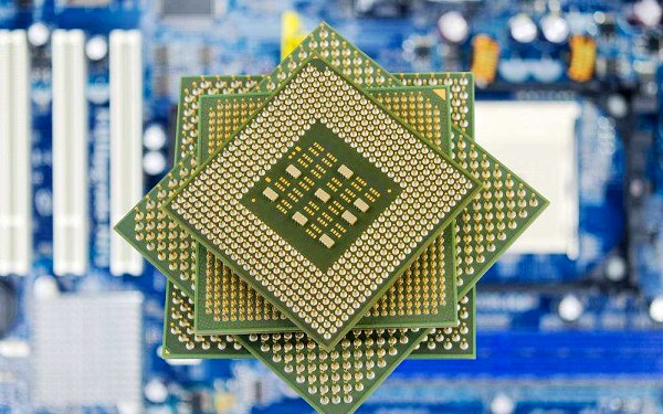
As electronic PCB products move toward miniaturization, portability, and high performance, higher requirements are placed on circuit assembly technology and I/O pin number. Chips volume are getting smaller and smaller and more and more pins which bring difficulties for production and repairing. In order to adapt to the rapid growth of the number of I / O, the new capsulation form - Ball Grid Array (BGA) was put into practical usage in the early 1990s.

Compared with QFP, the main feature of BGA is that the chip pins are not distributed around the chip, but on the bottom surface of the capsulation. In fact, the four sides of the capsulation substrate are turned into Pb-Sn bumps in the area array laying. Pins, I / O terminal spacing (such as 1.0m, 1.27mm, 1.5mm), can accommodate a large number of I / O; pin spacing is much larger than QFP mode, which improve yielda,bring high capsulation reliability, solder joints defect rate is low, the solder joint is firm; the centering and soldering are not difficult; the welding coplanarity is easier to guarantee than the QFP, and the reliability is greatly improved; the electric characteristics are better, and specially suitable for using in the high-frequency circuit: due to the small terminal, The self-inductance and mutual inductance of the conductor are very low, and the frequency characteristics are good. When re-flow welding, the tension between the solder joints produces a good automatic alignment effect, allowing 50% of the SMT accuracy error; the signal transmission delay is small, and the adaptation frequency is greatly improved; compatible with existing SMT crafts and equipment.
When the BGA is working, the chip temperature is close to the ambient temperature, and its heat dissipation is good. However, BGA capsulation also has certain limitations, mainly behave as the following: BGA post-weld inspection and maintenance is difficult, X-ray fluoroscopy or X-ray stratification inspection must be used to ensure the reliability of the solder joint, high equipment costs; easy moisture absorption, Drying should be done before usage.
The BGA usually consists of a chip, a pedestal, a pin and an capsulation shell. According to the position of the chip, it is divided into two types: the chip surface up and down; the pin arrangement is divided into ball grid arrays evenly distributed, the ball grid array Staggered distribution, ball array peripheral distribution, ball grid array with central heat dissipation and surrounding distribution of grounding points; classified by sealing method, divided into molded sealing and casting sealing; classified from heat dissipation angle, divided into heat-enhanced type, membrane cavity Down-type and metal ball grid array; According to the base material, BGA can be divided into plastic ball grid array PBGA (Plastic Ball Grid Array), ceramic ball grid array CBGA (Ceramic Ball Grid Array), ceramic column array array CCGA (Crystal) Columm Grid Array) and carrier ball array TBGA (Tape Ball Grid Array four.
 Building 1, Senyang Electronic Technology Park, Guangming High-tech Park, Yutang Street, Guangming District, Shenzhen City.
 F:86-13418481618
 pcba13@fastpcba.cn