About us
FASTPCBA Co.,Ltd
-
 Building 1, Senyang Electronic Technology Park, Guangming High-tech Park, Yutang Street, Guangming District, Shenzhen City.
-
 F:86-13418481618
-
 pcba13@fastpcba.cn
 date:2020-01-02 15:10:26

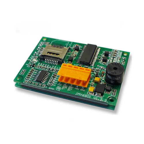
After the basic functions of electronic devices have been determined at the beginning of the design, the designer hands over the non-standard components to the fabs for fabrication, and the other standard components to the market. Once these custom components are made, they go through the wafer fabrication process to make parts suitable for assembly. The parts are then assembled and welded to the interface card or mother board (printed circuit board), which is a general electronic equipment production process.
The fabrication of wafers is defined as zero-order configuration, and the fabrication of wafers into a state suitable for assembly is called first-order configuration, the welding of components of first-order configuration to interface CARDS is called second-order configuration, and the motherboard of interface CARDS is called third-order configuration, which is the way the general electronics industry classifies the working class of overall electronic products. Therefore, for different electronic products, generally can be used to understand the point of view.
The overall electronic equipment with active components of the chip and many passive components as the smallest unit, these components with technological progress year by year high density, miniaturization, multi-functional. Although so-called system chips have long been an ideal, there are still difficulties in the practical world for more complex systems, so printed circuit boards still have to play the role of threading, again highlighting the fact that high-density components must be supported by high-density circuit boards.
From the bare crystal of the semiconductor to the closed particles or directly loaded onto the board, the more complex packaging particles are still installed on the printed circuit board after the closure, the interface card is also combined with the host board, although not all electronic devices follow the same pattern, but the general structure will be similar.
For example, mobile phones, video recorders, digital cameras, personal computers, and so on, all have similar structures but different complexity and density. As for the system products, such as the back board used in the communication room, that is another printed circuit board for a different purpose. Therefore, some people divide the circuit board into the so-called function board and interconnection board.
In recent years, due to the complexity of the integration of electronic equipment functions, the relative semiconductor configuration is also moving toward high position and high density, so the traditional wire configuration can no longer fully meet the needs of semiconductor configuration. Therefore, multi-grain module, bare grain direct loading, transfer plate configuration, chip size configuration, chip and configuration, needle array configuration PGA, ball array configuration, columnar array configuration and other configuration methods appear in different fields, and their connection to printed circuit board also presents a variety of changes.
The role of printed circuit boards is no longer just a platform for components. In most electronic configurations, higher-order plastic boards have begun to take on the task of high-density wafer assembly.
 Building 1, Senyang Electronic Technology Park, Guangming High-tech Park, Yutang Street, Guangming District, Shenzhen City.
 F:86-13418481618
 pcba13@fastpcba.cn