About us
FASTPCBA Co.,Ltd
-
 Building 1, Senyang Electronic Technology Park, Guangming High-tech Park, Yutang Street, Guangming District, Shenzhen City.
-
 F:86-13418481618
-
 pcba13@fastpcba.cn
 date:2019-07-05 11:24:00
Turnkey pcb manufacturing, layout design of reflow soldering surface components
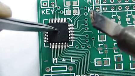
Reflow soldering has good craft performance, and there is no special requirements for the layout position, direction and spacing of components.The requirements of the solder paste printing stencil window to the component spacing, the space requirements for inspection and rework, and the craft reliability requirements are to be mainly considered for turnkey pcb manufacturing layout of the components on the reflow soldering surface.

1. For turnkey pcb manufacturing,surface mount components forbidden layout area.
A. conveying edge (edge parallel to the conveying direction), the distance from edge 5mm range is the forbidden zone. 5mm is a range that is acceptable for all SMT equipment.
B. Non-conveying edge (edge perpendicular to the conveying direction), 2~5mm from the side is the forbidden layout area. In theory, turnkey pcb manufacturing components can be laid out to the edge. However, due to the edge effect of the deformation of the steel mesh, it is necessary to set up a forbidden area of 2~5mm or more to ensure that the thickness of the solder paste meets the requirements.
C. Any kind of turnkey pcb manufacturing components and their welding pads cannot be laid out in the area where the conveying is prohibited. In the non-conveying edge prohibiting area, the layout of surface mount components is mainly prohibited, but if it is necessary to lay out the inserted components, the craft requirements of anti-wave soldering up to tin tooling should be considered.
2. Turnkey pcb manufacturing components should be laid out as regularly as possible.
The positive electrode of the polar component, the notch of the IC, etc. are uniformly placed upward and leftward. As the regular arrangement is convenient for inspection, which is beneficial to increase the speed of the mounting.
3. The turnkey pcb manufacturing components are laid out as evenly as possible.
Uniform distribution is beneficial to reduce the temperature difference on the surface of the reflow soldering, especially the integrated layout of large-size BGA, QFP, PLCC, which will cause local low temperature of the PCB.
4. The spacing (interval) between turnkey pcb manufacturing components is mainly related to the requirements of welding operation, inspection, and repair space.
For special needs, such as the installation space of the radiator and the operation space of the connector, please design according to actual needs.
5. Double-sided used reflow-welded turnkey pcb manufacturing boards (such as double-sided full SMD boards, mask-selectively welded double-sided panels) are usually the first to solder the large number and the lesser type of components (Bottom surface).
This surface is subjected to a secondary reflow soldering process in which components with few pins and relatively heavy and relatively high components cannot be placed. The general experience is a BGA device placed on a Bottom surface. The maximum gravity that the weld seam can withstand is 0.03 g/mm', and the remaining package is 0.5 g/mm'.
6. To avoid double-sided mirror mounting BOA design as much as possible.
According to relevant experimental research, the reliability of such design solder joints is reduced by about 50%.
7.Reflow soldering is supplied quantitatively, so punching holes in the pads should be avoided. Plating Over Filled Via (POFV) can be used if desired.
BGA, chip capacitors, crystal oscillators and other stress-sensitive devices should be avoided in the layout of the separation edge or near the bridge connection area, which places are easy to bend the PCB when assembling.
 Building 1, Senyang Electronic Technology Park, Guangming High-tech Park, Yutang Street, Guangming District, Shenzhen City.
 F:86-13418481618
 pcba13@fastpcba.cn