About us
FASTPCBA Co.,Ltd
-
 Building 1, Senyang Electronic Technology Park, Guangming High-tech Park, Yutang Street, Guangming District, Shenzhen City.
-
 F:86-13418481618
-
 pcba13@fastpcba.cn
 date:2021-07-29 14:13:47
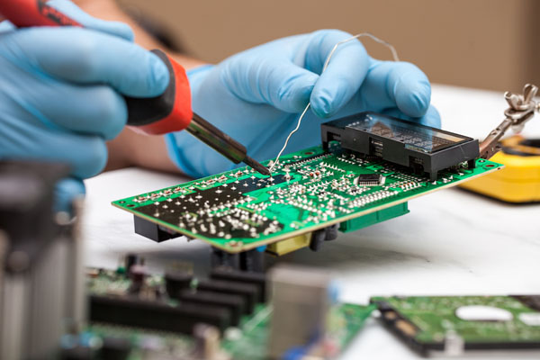
Soldering is an important process in PCB circuit boards. When we are making PCB, we often see many soldering defects.

Now FASTPCBA will explain to you what are the common soldering defects of PCB circuit boards:
1. Virtual soldering:
There is a clear black boundary between the solder and the lead of the component or with the copper foil, and the solder is recessed toward the boundary.
Hazard: The circuit board does not work properly.
Reason:
1) Leads of components are not cleaned, tinned or oxidized;
2) The printed circuit board is not clean, and the sprayed flux is of poor quality.
2. Solder accumulation:
The solder joint structure is loose, white and dull.
Hazard: Insufficient mechanical strength, possibly false welding.
Reason:
1) The solder quality is not good;
2) The welding temperature is not enough;
3) The leads of the components are loose.
3. Too much solder:
The solder surface is convex.
Hazard: Waste solder, and may contain defects.
Reason: The solder evacuation was too late.
4. Too little solder:
The soldering area is less than 80% of the pad, and the solder does not form a smooth transition surface.
Hazard: Insufficient mechanical strength of the circuit board.
Reason:
1) The solder fluidity is poor or the solder is withdrawn too early;
2) Insufficient flux;
3) The welding time is too short.
5. Rosin welding:
There is rosin slag in the weld.
Hazard: Insufficient strength, poor continuity, and may be switched on and off.
Reason:
1) Too many welders or have failed;
2) Insufficient welding time and insufficient heating;
3) The surface oxide film is not removed.
6. Overheating:
The solder joints are white, no metallic luster, and the surface is rough.
Hazard: The pad is easy to peel off and the strength is reduced.
Reason: The power of the soldering iron is too large and the heating time is too long.
7. Cold welding:
The surface becomes tofu-like particles, sometimes there may be cracks.
Harm: Low strength and poor conductivity.
Reason: The solder shakes before it solidifies.
8. Poor wetting:
The contact between the solder and the soldering interface is too large and not smooth.
Hazard: Low strength, unavailable or intermittently on and off.
Reason:
1) The weldment is not cleaned up;
2) Insufficient flux or poor quality;
3) The weldment is not fully heated.
The above is the analysis of the common soldering defects of PCB circuit boards. I hope everyone can avoid them in practice.
 Building 1, Senyang Electronic Technology Park, Guangming High-tech Park, Yutang Street, Guangming District, Shenzhen City.
 F:86-13418481618
 pcba13@fastpcba.cn