About us
FASTPCBA Co.,Ltd
-
 Building 1, Senyang Electronic Technology Park, Guangming High-tech Park, Yutang Street, Guangming District, Shenzhen City.
-
 F:86-13418481618
-
 pcba13@fastpcba.cn
 date:2018-04-27 09:29:00
What are the rules of the PCB layout in the state?
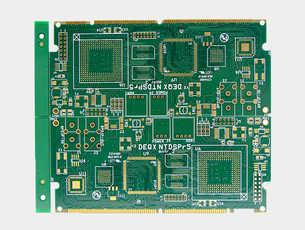
PCB board wiring is one of the important things that can't run. Pcb wiring is based on the electrical schematics and the wire table and the required wire width and spacing layout printed wire, wiring should generally follow the following rules:
1. On the premise of satisfying the requirements for use, the order of selecting the wiring method is single layer→first layer→multilayer, that is, the wiring can be simplified.
2. The signal on the same layer of the Pcb board changes direction with a ramp or a smooth transition, and the radius of curvature is a little better, to avoid electric field concentration, signal reflection and additional impedance.
3. The wiring layout between the two connection pads is as short as possible, and sensitive signals and small signals go first. To reduce the delay and interference of small signals. The grounding line shield should be laid next to the input line of the analog circuit; the layout of the same layer conductor should be evenly distributed. The conductive area on each wire should be relatively balanced to prevent board warpage.

4. Digital circuits and analog circuits should be separated in the wiring so as not to interfere with each other.
5. When the circuit components on the Pcba board are grounded and connected to the power supply, the traces should be as short as possible and as close as possible to reduce the internal resistance of the pcb board.
6. The lengths of the I/O lines of high-speed circuits, such as multiple I/O lines and differential amplifiers and balanced amplifiers, should be equal. To avoid unnecessary delay or phase shift.
7. The traces on each layer of the multilayer board should be perpendicular to each other to reduce the coupling. Avoid alignment and balance of the upper and lower layers.
8. When the pad is connected with the conductive area of large and small area, it should be insulated with a thin wire with a length of not less than 0.5mm. The width of the thin wire should not be less than 0.13mm.
9. The wire closest to the edge of the printed circuit board should be greater than 5mm from the edge of the printed circuit board. The ground wire can be close to the edge of the board when required. If a guide rail is to be inserted during the processing of a printed circuit board, the distance between the wire and the board must be at least greater than the depth of the guide rail.
FASTPCBA Technology Co., Ltd is a professional PCB manufacturer in China, Shenzhen. With 14 years of development, FASPCBA turns into a first class manufacturer of HDI PCB, with production capability 35,000 square meters.If you want to learn more PCB, please contact: pcba23@pcb-smt.net
 Building 1, Senyang Electronic Technology Park, Guangming High-tech Park, Yutang Street, Guangming District, Shenzhen City.
 F:86-13418481618
 pcba13@fastpcba.cn