About us
FASTPCBA Co.,Ltd
-
 Building 1, Senyang Electronic Technology Park, Guangming High-tech Park, Yutang Street, Guangming District, Shenzhen City.
-
 F:86-13418481618
-
 pcba13@fastpcba.cn
 date:2021-12-08 15:19:30
Generally, there are problems in the manufacturing process of printed circuit boards that can cause printed circuit errors due to the following factors:
* Defects in the metallization process that must be conductive inside the perforation.
* Undesirable copper bumps and islands between conductors will affect their insulation.
* Resistivity will affect the pollution of the PCB by the insulating material between the conductors.
* An accident occurred during the process after the last AOI inspection procedure, and it will cause a short circuit or open circuit.
Why PCB Need Electrical Testing?
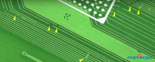
Through the electrical continuity and insulation test of the PCB circuit board, it can be ensured that the PCB is free of defects before assembly, which prevents the possible short circuit or open circuit in the printed circuit.
Which standard is suitable for this type of test?
The specifications that must be met for this type of printed circuit test are governed by the IPC9252 standard.
What is the grid on the PCB?
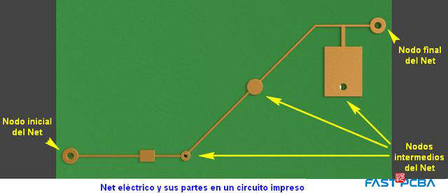
We usually hear this term in our electronic design software. The network on the printed circuit is a set of points, which are electrically connected to the start and end points through the trajectory we designed. It includes component pads, traces, test points (if any) and copper planes associated with the same connection, as shown in the following figure:
What is a netlist?
It is a term used to describe an alphanumeric list that represents a connected group of two or more points that have common electrical characteristics in a printed circuit.
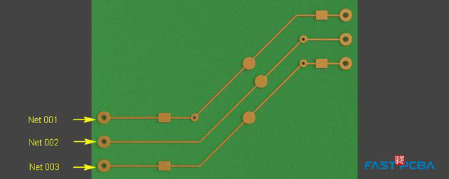
Most electronic design programs generate a web list that contains a description of the electrical connections between the different components of the printed circuit. See the description below:
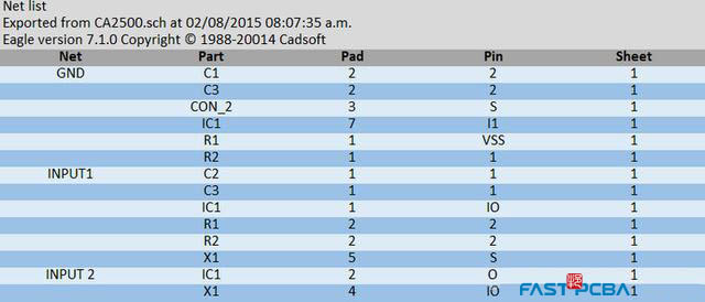
The printed circuit manufacturer will extract this connection list from the Gerber file that we send for its manufacturing, so that the electrical test process can be carried out on our board.
What is a 100% net list test.
In the case of a multi-layer card, this is an electrical test performed on each node of the card and all networks of the card (including its external and internal copper layers).
Basic standards for electrical testing process
Any pad found on the PCB by the solder mask must belong to the test pad of a certain component or circuit. In both cases, it is necessary to check their electrical conductivity and electrical isolation from other pads and the traces connecting them. Usually, the information is extracted by the manufacturer that provides this service from the following files sent by the customer to the production:
Gerber file, corresponding to the solder mask. Need to determine where the test leads should be placed.
Drill files. Its processing can accurately calculate the available copper area around the perforation, thereby preventing the test lead from entering and destroying it or generating errors.
Copper layer file. Outside, top and bottom, and inside (if any).
The electrical test system uses this information to extract a list of electrical networks corresponding to our card, so that it can verify its integrity based on conductivity and insulation.
How to implement this type of testing in practice?
There are basically two ways to perform this process:
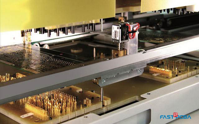
Needle-bed test: This type of test is usually called "bed-of-needle test". The method is to place the card on a frame that has many retractable pins that are in contact with the same number of pads on our card. The connection is connected to an interface that performs the different continuity, capacitance and insulation measurements required by the program. This process is aimed at large-scale production, in which case putting the product on the market requires rapid production of printed circuits for assembly.
The image below shows two cards mounted on an aluminum frame, and then down into the test needle bed at the bottom of the machine to perform the above process.
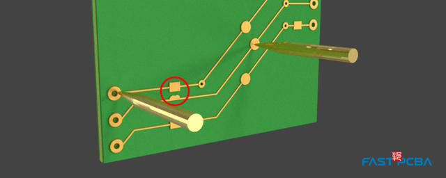
Flying probe electrical test: In this process, the card is placed vertically in the frame, and the test probes are moved along the XY direction on both sides of the circuit to accurately place them on the pads whose electrical characteristics are to be tested. Then, the test wires move on the Z axis until they make contact with the pads, as shown in the figure below, allowing the software to perform the required measurements and display the results of determining whether the card is passed or rejected. (fail).
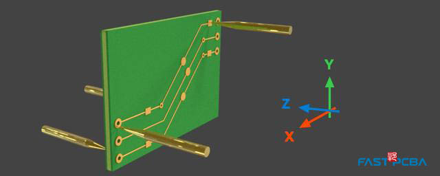
For all networks that make up the printed circuit, repeat the above sequence at the speed allowed by the system to ensure that we only receive electrically reliable cards for later assembly.
Today’s printed circuits require this state-of-the-art technology to perform this process. In this process, high-precision CNC systems are combined to allow the test line to be accurately positioned on the current fine pitch pad of 0.2mm wide. superior.
What types of tests are performed during electrical testing?
Capacitance test: This test is designed to detect the open trajectory of the universal card and part of the main card without error, and measure the capacitance by applying charge to reflect the capacitance in different Nets, and compare its value with the card under test to generate a measured value that is different The list of corresponding points.
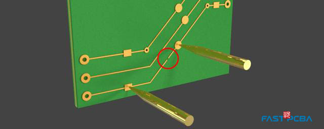
Continuity test: This test is designed to detect short circuits between the different networks that make up our card to ensure that no current flows between them.
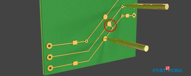
Insulation test: The chemical manufacturing process of printed circuit boards may eventually leave small copper residues, which may or may not adhere to our card nets, and will not indicate a real short circuit between them. But it will shorten the separation distance of its original design. The test is designed to detect these problems between different networks to ensure that their insulation is high enough to avoid unnecessary electrical interactions (for example, voltage jumps or current leakage).
What voltage is applied for the insulation test?
The electrical test system applies a voltage between 30 and 100 volts to the card's network to sense the voltage jump caused by the residual copper layer, which violates the minimum distance designed by the user between different networks.
Contact FASTPCBA
FASTPCBA CO., LTD. produceds printed circuit boards that are vigorously tested for quality and accuracy by skilled, dedicated quality assurance professionals with high-level testing equipment. To understand how FASTPCBA provides high-quality PCBs to industries around the world, or learn about your For PCB project questions, please contact us immediately.
 Building 1, Senyang Electronic Technology Park, Guangming High-tech Park, Yutang Street, Guangming District, Shenzhen City.
 F:86-13418481618
 pcba13@fastpcba.cn