About us
FASTPCBA Co.,Ltd
-
 Building 1, Senyang Electronic Technology Park, Guangming High-tech Park, Yutang Street, Guangming District, Shenzhen City.
-
 F:86-13418481618
-
 pcba13@fastpcba.cn
 date:2021-07-02 17:29:19
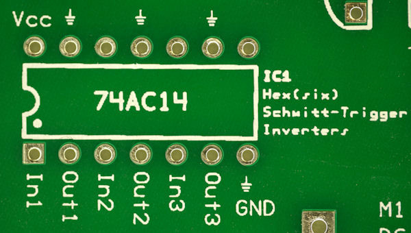
Circuit board screen printing is the use of screen printing technology to make printed circuit boards. The silk screen value is the silk screen layer. When drawing the pcb, it is layered. The layer containing the text is used to mark components or add other information. This layer is called the silk screen layer.

The component shape, serial number, and other descriptive text are printed on the component surface or soldering surface by screen printing to facilitate the plug-in (including the surface-mounted component patch) of the circuit board production process and the maintenance operation of the product in the future.
The silk screen layer is generally placed on the top layer, but for electronic products with a high failure rate and frequent maintenance, such as the motherboard of TVs, computer monitors, printers, etc., a silk screen layer can be set on the component surface and the solder surface.
The importance of PCB screen printing
It is not an exaggeration to compare the PCB screen printing to the outerwear of the PCB board. As the saying goes, people rely on clothing, so having a good-looking appearance is the most intuitive experience for users to look at the printed board. Users will comment on a board because of its appearance. In addition, the silk screen solder mask and characters are the post-processes in the lengthy manufacturing process of the printed board. The printed board that is about to be completed with a high value has errors in the post-process, and the loss is too large. It's not worth it. Besides, solder mask and characters are one of the processes with the largest amount of scrap. Therefore, it is very important to stabilize the process of screen printing solder mask and characters, and straighten out the management of this process, document control and equipment maintenance. Up.
After 1990, basically all PCB factories did not use traditional craftsmanship. There are reasons for this, including: the density of double-sided and printed boards is increasing. The high density of small holes and fine lines SMT is an irreversible trend in the development of printed boards. The line width spacing is 0.12~0.20mm narrow welding. The ring is already in the majority, and the silk-screen thermosetting green oil is powerless, the appearance is not neat, the oil is leaked on the pad, and the printing is too much affected by the proficiency and emotions of the silk-screen employees. Therefore, most of the current double-sided and multilayer board factories All have eliminated the thermosetting epoxy green oil and switched to the liquid photosensitive solder mask process.
 Building 1, Senyang Electronic Technology Park, Guangming High-tech Park, Yutang Street, Guangming District, Shenzhen City.
 F:86-13418481618
 pcba13@fastpcba.cn