About us
FASTPCBA Co.,Ltd
-
 Building 1, Senyang Electronic Technology Park, Guangming High-tech Park, Yutang Street, Guangming District, Shenzhen City.
-
 F:86-13418481618
-
 pcba13@fastpcba.cn
 date:2021-11-26 17:15:53
In recent years, area array components such as BGA, QFN, CSP and flip-chip have become more and more widely used in the field of electronics manufacturing. For example, BGA, compared with other components, has many pins, smaller inductance and capacitance between pins, and better heat dissipation performance. However, BGA also has disadvantages. For example, after SMT, it is difficult to judge the solder joints under the package through visual inspection or AOI test.
X-ray equipment is based on the strong penetrability of X-rays. The light tube emits X-rays under high pressure, which can effectively penetrate the object to be measured. The image performance changes due to the difference in density and thickness, thereby realizing solder joint detection. In order to ensure welding quality, more and more manufacturers choose to use X-rays to inspect components that hide solder joints.
How to use X-ray inspection?
The X-rays emitted by the automatic X-ray transmission tube pass through the test sample. The detector is located on the other side of the AXI machine. The detector converts X-rays into visible light and provides optical images from the camera. The sample material absorbs X-rays to varying degrees due to its own density and atomic weight. Therefore, the imaging on the receiver will be significantly different, the higher the density, the stronger the absorption of X-rays, so the shadow image is clearer. The closer you are to the X-ray tube, the larger the image; the farther you are from the X-ray tube, the smaller the image.
What defects can be detected by X-rays?
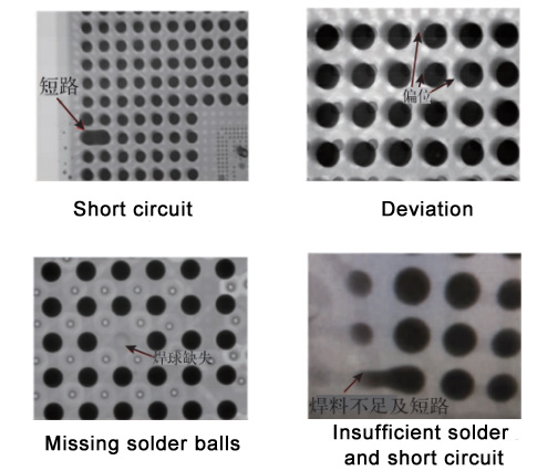
X-rays can detect the internal conditions of component welding. It uses the penetrating power of X-rays to detect insufficient solder, poor solder, solder shorts, and other problems with solder joints.
When there are defects such as voids, slag inclusions and incomplete welding, the defect area will form bright spots or bright lines. Visually, we can judge whether a certain area in the defect detection image is brighter than the surrounding background area to determine whether the area is a defect. From the perspective of image processing, we can determine whether the area is a defect based on the gray value of the pixel in the defect detection image.
The most likely cause of voids is the solder paste and the component itself. In the X-ray image, some "bubbles" can be seen in the solder joints.
If there is a gray "bridge" between the solder joints, we can basically judge it as a solder short circuit.
If the amount of solder paste is abnormal or SMT deviation, the component may shift. According to the X-ray inspection image, the shadows of the pins and pads do not match, and it can be found that the components are misaligned.


*Poor welding can be determined by the gray scale and size of the joint.
Oxidation of PCB pads can cause poor soldering. The image displayed by X-ray inspection is that the solder joint is significantly larger than the normal solder joint.
During reflow soldering, the solder paste is insufficient or the solder paste flows into nearby through holes. On the X-ray image, the solder joints are smaller than normal.
Due to insufficient soldering temperature and time during reflow soldering, the SMT solder paste is not completely fused, resulting in cold soldering. It is usually difficult to find, but the X-ray inspection image clearly shows the problem.
 Building 1, Senyang Electronic Technology Park, Guangming High-tech Park, Yutang Street, Guangming District, Shenzhen City.
 F:86-13418481618
 pcba13@fastpcba.cn